|
|
To generate accurate structures photo lithography is used. Here, a UV light sensitive photo resist is irradiated through a glass mask on which an opaque chromium layer is located to transfer the structures onto the substrate. Depending on the type of photo resist the exposed or unexposed areas of resist are then developed in a developer solution. In subsequent processes the structures can be transferred into underlying layers or layers of metal can be deposited within the resist structures. |
|
Positive / Negative Photo lithography
Typically, we use positive and negative lithography with resist thicknesses between 0.2 µm and 10 µm. In positive lithography the UV exposed areas of the resist are soluble in the developer. In the negative lithography, the photo resist is stabilized by the exposure and the unexposed areas remain soluble in the developer. The developed surfaces are then accessible for etching or deposition processes.
Typical properties:
- Smallest feature: about 0,5µm
- Resist thickness: 0,2 µm - about 10 µm
|
|
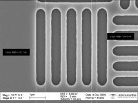 |
Resolution test pattern |
|
Lift-off lithography:
Lift-off lithography uses photo resists that generate a negative sidewall profile. To strengthen the effect also double coating systems can be used. The bottom photo resist is than developed a bit underneath the upper photo resist. Subsequent coating processes do not cover the undercuted side walls completely. Upon removal of the photo resist the layer which is located on the photo resist is lifted together with the photo resist. This method allows the structuring of materials that can not be etched easily, such as noble metals.
Typical properties:
- Smallest feature: about 0,7 µm
|
|
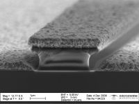 |
Lift-off resist coated with Zn/Ti film
|
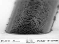 |
Zn/Ti after lift-off step |
|
Thick film lithography:
To manufactured electro deposited metal parts, photo resist forms are used in which a metal layer is deposited electrochemically. Since the thickness of the photo resist is the limiting factor for the thickness of the metal layer, coatings are used which allow largest possible resist thicknesses. With the negative photo resist SU-8 structure heights of several 100 microns are available. With positive resists which are easily soluble structure heights up to some 10 microns are possible, with also almost vertical side walls.
Typical properties:
- Feature hight: up to about 1mm
- Aspect ratio: 10:1
|
|
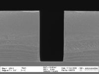 |
Cross section of an SU-8 trench |
|
Lithography over topography:
Manufacturing of MEMS devices often requires additional lithography steps over existing topography. This for example is the case when electrode structures are to be performed on thin membrane surfaces. We use special photo resist coating processes, to get a good coverage of oblique or even vertical side walls.
Typical properties:
- Topography at vertical edges: some 10 µm
- Topography at oblique edges: some 100 µm
|
|
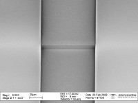 |
Lithography over 10µm high step |
 |
Gold feature over 10µm high step |
|
Aligned Lithography:
For production of microcomponents often multiple lithography steps are required. It is necessary that the individual lithography steps are aligned with one another as well as possible.
Typical properties:
- Maximum alignment accuracy: 0,5-1 µm
|
|
|
|
|
Double sided Lithography:
For double sided processing of substrates, for example when back side holes are to be positioned regarding to front side structures, double sided lithography is used. Here also, the best possible adjustment of the rear to the front side lithography structures is necessary.
Typical properties:
- Maximum alignment accuracy: ~1 µm
|
|
|
|
|
|